
Paul Johns, PhD
Research Chemist. Ultrafast Spectroscopy.
Transient absorption microscopy studies of single metal and semiconductor nanostructures
Proceedings of SPIE, Conference Volume 9549, Physical Chemistry of Interfaces and Nanomaterials XIV, 954914.
Publication year: 2015
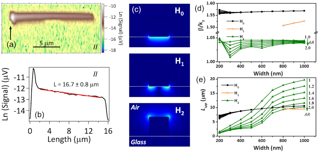
Transient absorption microscopy is an experimental technique that allows nanomaterials to be studied with ultrafast time resolution and diffraction limited spatial resolution. This paper describes recent results from using transient absorption microscopy to investigate energy relaxation processes in single metal and semiconductor nanowires. The processes that have been examined include charge carrier trapping in semiconductor nanostructures, the motion of surface plasmon polaritons in metal nanowires, and the damping of the acoustic breathing modes of metal nanowires by high viscosity solvents.
Leave a Reply